High-Resolution 3D-Printed Stamps for Printing Electronics
Electronic components can also be manufactured by roll-to-roll processes, where a special stamp transfers the printing material to the substrate. However, common defects, such us haloing or bridging, negatively affect the performance of printed materials for electronics applications.
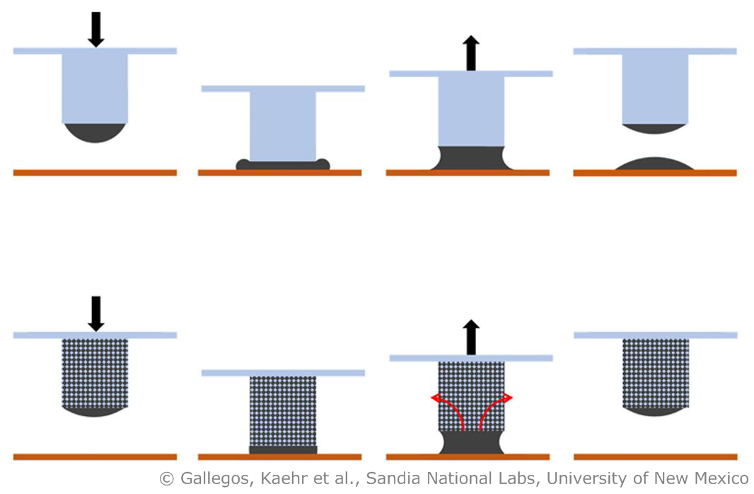
To solve this problem, researchers around Michael Gallegos from Sandia National Laboratories and The University of New Mexico (US) work on a new approach: 3D-printed mechanical metamaterials for metered ink deposition. These porous stamps use capillary forces during mechanical deformation to enable metered material transfer. One of the main drawbacks in roll-to-roll processes is the excess amount of ink left on the substrate after lifting off the stamp creating aforementioned defects. Therefore, the researchers aim at making the material dispense more controllable.
They used a Nanoscribe 3D printer to fabricate stamps with micrometer-sized pores. In the stamping process, the pore-space acts as the reservoir and the mechanical deformation as the “metering pump”. When using a porous stamp, suction force pulls the ink back into the stamp when lifting it off. This way, ink overspill can be avoided. Moreover, the researchers printed fibrous stamps to compare to solid stamps. They found that regardless of the density of fibers, fibrous stamps printed with greater fidelity as well as more uniform film thickness versus solid stamps.
This work with regards to fluid mechanics opens up many applications, e.g., for cost-effective, ubiquitous sensors. At MRS Fall 2018, the team even won the Best Poster Award for their work.